+86-1478258894512522120
葩星12522120 淘宝旺旺passiontechinc

pt@ptinfous.com

+86-14782588945

  加载中,请稍候...
浏览历史


RTDAC_板卡_Reconfiguration

关键词: RTDAC_板卡_Reconfiguration


简介:InTeCo Ltd. Re-configuration ul. Lea 203 30-150 Kraków of the RT-DAC4/PCI and Poland E-mail: inteco@kki.krakow.plRT-DAC/USB boardshttp://www.inteco.com.pl 2004-10-10Hardware functions changed by software Do you need a PCI or USB boardequipped with a unique number andtype of I/O channels? We can program (re-configure) anRT-DAC PCI or USB device for you.Or e...
品 牌 inteco inteco
产 地 波兰
型 号 PXF3295
折 扣 其他电询
咨询专家:

黄工-工业总线-工业自动化-实时仿真

黄工-工业总线-工业自动化-实时仿真 ID:2937

   机电电子工程专业硕士,机械设计制造及其自动化/计算机双学士,高级工程师

    具有丰富的从业、管理经验,曾在机电工程公司,资深设计代理公司工作。历任组织、经理等岗位,同时具有深厚的理论基础和项目项目研发经历。...

[MORE]

赵工-总线系统-嵌入式系统-工业自动化

赵工-总线系统-嵌入式系统-工业自动化 ID:2940

    机械电子工程,嵌入式系统专家,高级工程师

    嵌入式项目开发,ARM,Freescale,Infilion等系列单片机系统开发,DSP嵌入式系统开发,FPGA系统开发,项目经验丰富。


...

[MORE]

产品说明:

inteco Ltd.

Re-configuration

ul. Lea 203 30-150 Kraków

of the RT-DAC4/PCI and

Poland

E-mail: Inteco@kki.krakow.pl RT-DAC/USB boards http://www.inteco.com.pl

2004-10-10 Hardware functions changed by software

Do you need a PCI or USB boarequipped with a unique number antype of I/O channels?

We can program (re-configure) aRT-DAC PCI or USB device for youOr even you can do it yourself! And yodo not need to change the hardware!

The RT-DAC PCI and USB devices contain an FPGA circuit connected to all digital I/O signals as well as to the control signals of the A/D and D/A converters. The FPGA chip is the master controller of the board resources. The number of the digital and analog I/O channels in the PCI and USB devices is given in the table below.

Digital I/O Analog inputs Analog outputs
RT-DAC4/PCI 52 16 4
RT-DAC4/PCI-D 92 - -
RT-DAC/USB 26 16 4
RT-DAC/USB-D 26 - -

The number of the digital and analog I/O channels is fixed but their functions are fully determined by the FPGA configurationTHE BOARDS ARE RECONFIGURABLE NOT JUST PROGRAMMABLEThe configuration phase determines the hardware functions of the board resources. After configuration the functions of the board are accessible in a programming manner as in the case of other “typical” boards. The re-configuration does not require any hardware changes. Either in the case of

RT-DAC/PCI as well as RT-DAC/USB the re-configuration requires only to start a dedicated programs. The inputs of the re-configuration programs are configuration files that define the logical structure of the FPGA circuit. The configuration files may be created by a user. A number of configuration files is distributed by Inteco as well. If one uses a configuration file the hardware functions of the PCI or USB device may be changed. The point is that the re-configuration changes hardware functions. Typically the hardware functions of the boards are fixed and behaviour of the boards is determined by the software. The hardware functions of the RT-DAC devices may be customized and finally, as in the case of “typical” boards, the board resources are managed by a software.

The configuration of FPGA can be redesigned introducing a new functionality. The new FPGA configurations can be developed by a board user or by the development team of Inteco. In the first case the user does need the “FPGA Programming Guide” that covers all aspects required to utilize board resources. The short description of the typical FPGA blocks applied in the board configuration designs is given below (a new blocks can be developed on a request). A number of blocks can be included into a single board configuration up to the capacity of the FPGA chip. The different configurations can be loaded to the board unlimited number of times. The board reconfiguration is controlled by the dedicated software and none hardware changes are required.

EXAMPLE: Let us consider the default RT-DAC4/PCI-D configuration which contains:

  • 86 general purpose digital I/O signals,
  • 4 PWM outputs,
  • 4 incremental encoder inputs,
  • 2 32-bit timers,
  • 2 32-bit counters
  • 2 digital signal generators and
    • PCI interrupt controller.
    • Let us assume that timers, counters and signal generators are not required in a new application. But there are 12 incremental encoders required instead of 4 encoder channels available in the default configuration. If the RT-DAC4/PCI-DOMNI board is used such a functionality change can be done without any hardware changes. The new FPGA configuration has to be designed by a user or ordered from Inteco. The new FPGA configuration can be applied which turns RT-DAC4/PCI-D into a new board. After the re-configuration the board I/Os may look as follow:
  • 86 general purpose digital I/O signals,
  • 4 PWM outputs,
  • 12 incremental encoder inputs,
  • 2 32-bit counters
  • PCI interrupt controller.

If the initial I/O channels are required the reconfiguration can be performed once more to switch the functions back to the initial state. As well any other I/O channels may be introduced and implemented in the FPGA hardware.

Below are presented the main features of the most popular blocks used to develop customized PCI and USB board configurations. They are a kind of bricks used to build FPGA configurations. Of course a new block functions may be develop on request.

Programmable general-purpose input and output digital signals.

FEATURES:
  • Up to 52 general purpose I/Os of RTDAC4/PCI, up to 92 I/Os of RT-DAC4/PCI-D and up to 26 I/Os of RT-DAC/USB
  • Individual selection of the direction of each I/O
  • LVTTL voltage levels
  • Change-Of-State (COS) PCI interrupt

CUSTOMISATION: functions associated with the I/O signals, the number of inputs associated with the COS interrupt. User defined functions can be associated with the I/O signals, for example an acquisition of binary signals or generation of digital signal patterns.

Interface to the incremental encoder sensors.

Operation of the quadrature encoder counter.

FEATURES:
  • 32-bit encoder counter
  • Software or hardware reset signal
  • Disable reset signal flag
  • Selection of the level or edge of the reset signal
  • Optionally the index signal can be applied to reset the counter

CUSTOMISATION: the number of available blocks, the length of the encoder counter and the assignment to the board pins.

Block diagram of the PWM generator.

FEATURES:
  • Selection of the prescaler and duty cycle values
  • 12-bit or 8 bit duty cycle resolution
  • 16-bit reference signal prescaler

CUSTOMISATION: the number of available blocks, the length of the block counters, duty cycle resolution and the assignment to the board connectors.

Generation of a number of periods of a digital signal.

Parameters of the digital signal generator wave.

FEATURES:
  • Generation of the defined or infinite number of periods
  • Selection of the beginning and termination period states
  • Independent selection of the length of the beginning and end period states

(the duty cycle and frequency

selection)

  • 32-bit counters for the number of periods and for the length of the beginning and end period states
  • Software or hardware trigger signal
  • Selection of the trigger signal edge
  • Pre-trigger and post-generation signal level selection
  • PCI interrupt generation at the termination of the generated wave

CUSTOMISATION: the number of available blocks, the length of the block counters and the assignment to the board pins.

Pulse Width Modulation (PWM) signal generator. This block is the scaled-down version of the digital signal generator block. The block generates PWM waves dedicated to the DC drive control.

Width measurement of the signal defined by the start and stop signals.

FEATURES:
  • 25 ns resolution
  • 32-bit time reference counter
  • 32-bit pulse with counter
  • Single start/stop signal or separate start and stop inputs
  • Hardware or software start and stop signals
  • Selectable edge or level of the start and stop signals
  • Gate signal
  • Real-time clock function
  • PCI interrupt generation at the end of measurement

CUSTOMISATION: the number of available blocks, the length of the time reference and pulse width counters and the assignment to the board pins.

• Single or continuous measurement mode

CUSTOMISATION: the number of available blocks, the length of the time reference and pulse counters and the assignment to the board pins.

The block operates in two modes and can be applied to measure the frequency or the pulse width of the input signal.

In the frequency measurement mode the block counts the impulses of the input signal.

The block count the number of input pulses within a given time period.

FEATURES:
  • 32-bit timing reference counter
  • 25 ns timing resolution
  • 32-bit input pulses counter
  • Hardware or software start and stop signals
  • Selectable edge or level of the start and stop signals
  • Gate signal for timing counter and/or for input pulses
  • PCI interrupt generation at the end of measurement

Principle of the frequency operating mode.

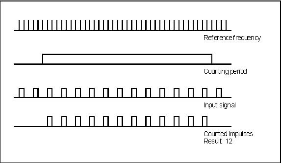
The counting period can be defined in a programming manner. The resolution of the counting period is 25 ns. The counting may be started by a program or by an external signal.

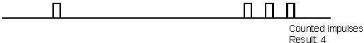
The block counts the rising edges of the input signal. If it is needed to count the falling edges a program can invert the input signal at the input of the block.

Optionally a gate input signal can be applied to stop the counting of the pulses of the input signal as well as to stop the counting of the counting period. The source of the gate signal may be a program or an external signal. The active level of the gate signal may be set by a program.

Reference frequency

Counting period

Input signal

Gate signaActive high

Principle of the gate signal.

When the counting period terminates the result is ready. Optionally a PCI interrupt may be generated at counting completion.

In the pulse width mode the block counts the time span between the start and stop conditions. The resolution of the time measurement is 25 ns. The start and stop conditions are selected in a programming way as rising or falling edges of the input signal. So the block may be applied to measure the duration of the “H” input state (start signal generated by the rising edge and stop generated by the falling edge), the duration of the “L” state of the input signal (start and stop conditions generated by the falling and rising edges respectively) or to measure the period of the input wave (both stop and start signals generated by the rising or falling edges).

The counting may be gated as in the case of the frequency measurement mode. As well a PCI interrupt may be optionally generated when the counting is completed.

The FreqM block is implemented as a Finite State Machine (FSM). The FSM contains four states: DisabledTriggeredCounting and Ready. The state flow is presented below.

Counting period

Start signal

Stop signal

Principle of the period measurement.

Current state of the FSM may be read by a program.

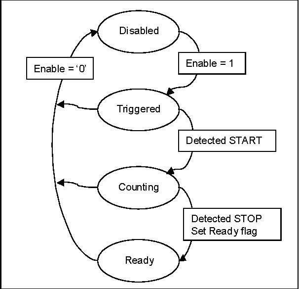
FSM of the FreqM block.

If the Enable flag is cleared the block remains in the Disabled state. When the Enable changes from 0 to 1 the state changes to Triggered. In the Triggered state the blocks waits for the start counting condition. In the frequency measurement mode the start condition comes from the software or hardware start signal. In the pulse width measurement mode a proper edge of the input signal has to be detected to generate the start counting signal. After the start counting condition appears the blocks moves to the Counting state. In the frequency mode the block counts the periods of the input signal and in the pulse width mode the clock periods are counted. The block switches into the Ready state when the stop condition is detected. In the frequency mode the stop condition is generated if the timer reaches zero value.

In the pulse width mode the stop is generated by a proper edge of the input signal.

CUSTOMISATION: the number of available blocks, the length of the time reference and pulse counters and the assignment to the board connectors.

Generation of the PCI interrupts. This function is not available for USB devices.

FEATURES:
  • Software interrupt source
  • Timer interrupt; 32-bit timer counter; 25-ns resolution
  • External interrupt sources
  • Interrupt sources from the configuration blocks

CUSTOMISATION: the number and source of the interrupt signals, assignment of the external interrupt sources to the RT-DAC4/PCI board pins.

Fast acquisition of the binary signals.

FEATURES:
  • Software or hardware acquisition start and stop signals
  • Trigger signal (a given appearance of given signal states)
  • Pre-trigger signal acquisition
  • 25-ns minimum acquisition internal period
  • Acquisition in the on-board 48 kbit dual-port memory
  • Gate signal
  • Interrupt generation at the end of the acquisition

CUSTOMISATION: the number and acquired signals, the assignment of the control and acquired signals to the board pins.

Acquisition of the binary signals in a FIFO queue.

FEATURES:
  • Software or hardware acquisition start and stop signals
  • Trigger signal (given appearances of given signal states)
  • Pre-trigger signal acquisition
  • Acquisition in the on-board FIFO memory (48 k bit capacity)
  • Gate signal
  • Interrupt generation when a number of FIFO elements exceeds a given value

CUSTOMISATION: the number of acquired signals, the assignment of the control and acquired signals to the board pins.

Acquisition of the analog signals in a FIFO queue.

FEATURES:
  • Software or hardware acquisition, start and stop signals
  • Trigger signal (an analog signal crosses a given level)
  • Pre-trigger signal acquisition
  • Acquisition in the on-board FIFO memory (48 k bit capacity)
  • Gate signal
  • PCI interrupt generation when a number of FIFO elements exceeds a given value

CUSTOMISATION: the number of acquired signals and the assignment of the control signals to the board pins.

Generation of 4 analog signals from a FIFO queue.

FEATURES:
  • Software or hardware generation, start and stop signal
  • On-board FIFO memory (48 k bit capacity) applied to store the shape of the generated waves
  • PCI interrupt generation when a number of FIFO elements falls below a given value

CUSTOMISATION: the number of generated waves and the assignment of the control signals to the board pins.

Others blocks can be designed on a request. The only limit is the capacity of the on-board FPGA circuit.

Revision History

Version Date Resp. Description
1.0 04-10-10 KK First release
inteco
参数资料:
RTDAC_板卡_ReconfigurationRTDAC_板卡_Reconfiguration
该文章系原厂商文章翻译,不通之处请参考原文
价格列表: RTDAC_板卡_ReconfigurationRTDAC_板卡_Reconfiguration
葩星订货号 订货号 产品名称 报价 品牌  
相关产品: RTDAC_板卡_ReconfigurationRTDAC_板卡_Reconfiguration
  咨询历史: